PCB Anatomy
The layered board that ties every chip together. Learn to read its traces, vias, pads, and silkscreen before you touch a probe, because the board itself is your first recon report.
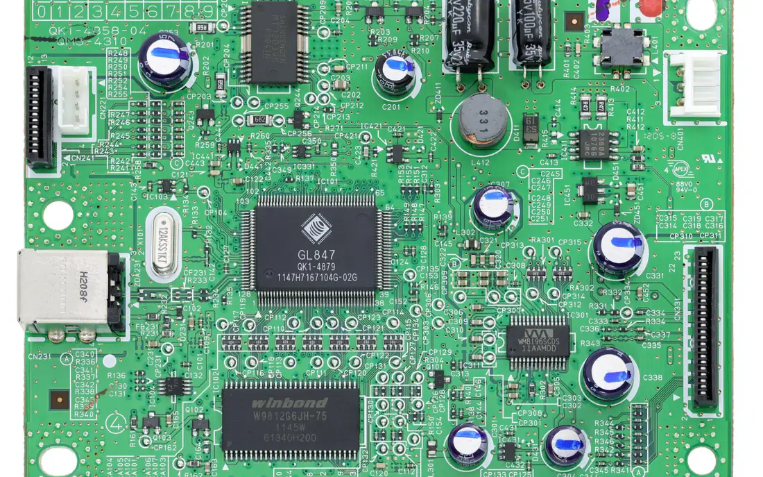
A PCB (printed circuit board) is the layered fibreglass board that mechanically holds a device's components and electrically connects them with etched copper. Reading a PCB is the first move of any hardware assessment: before you clip a single probe, the board's own layout tells you where power, the data buses, and the debug interfaces live.
What it is
The base is FR-4, a glass-epoxy laminate, with copper layers etched into traces and bonded together by insulating prepreg. A simple gadget uses two copper layers (top and bottom); denser designs stack four, six, or more, with internal ground and power planes sandwiched inside (see the diagram). Every visible feature has a name and a meaning:
| Feature | What it is | Why you care |
|---|---|---|
| Trace | Etched copper line carrying one signal | Follow it to see what connects to what |
| Via | Plated hole linking layers | A signal you lose on top may resurface on the bottom |
| Pad / test point | Exposed copper for probing | Where you actually clip on |
| Silkscreen | Printed white labels (TP1, RX, J2, U3) |
Free hints from the designer |
| Header / footprint | Row of holes or pads for a connector | Often the UART or JTAG you are hunting |
| Ground plane / pour | Large copper fill | Your reference ground for continuity |
Why it matters
The people who built the board left evidence all over it. Silkscreen may spell out RX/TX/GND next to a header, label a JTAG block, or number test points that the factory used for programming. A component's package and size tell you which chip is the main SoC and which is the flash. Trace routing shows which pads connect back to that SoC. All of this is recon you get for free, from a photograph, before any tool touches the board.
How you read one
- Photograph both sides in good, raking light and zoom in on the silkscreen. High-resolution photos are a lab notebook you can annotate later.
- Identify the big parts. The largest chip is usually the MCU/SoC; a nearby 8-pin part is often the SPI flash. Read the markings and pull the datasheets.
- Trace candidate interfaces. Follow four-pin headers and lone test points back to the main IC; a group of pads routing straight into the SoC is a strong UART or JTAG candidate.
- Buzz it out. With a multimeter in continuity mode (board off), confirm which pad is
GNDagainst a ground plane, then findVCC, and only then bring in a logic analyzer or UART adapter.
Pitfalls
- Silkscreen lies (or is absent). Labels are a hint, not gospel; footprints get reused and boards get re-spun. Always confirm a pin electrically before you trust the print.
- Inner layers are invisible. A trace that vanishes into a via may run through a hidden layer; you cannot follow every net by eye on a multilayer board.
- Ground is a plane, not a pin. On a dense board almost any large copper fill is ground; use it as your continuity reference rather than hunting for one magic
GNDpin. - Test points are not always live. Factory programming pads may be disabled or unpopulated in production; presence of a pad does not guarantee an open interface.
Further reading
Used in these courses
You have a firmware blob. What now? This course teaches the complete analysis workflow: identify the format, extract the filesystem, explore the structure, and find what matters. Every IoT device has firmware - this is how you read it.
U-Boot Debug Header Secrets**Beginner** probe lab. Clip onto a U-Boot serial console, find the non-default baud, dump the bootloader environment to leak a provisioning secret, then read the fused OTP key and unlock the secure region. Model B: bring your own probe CLI, flags travel over the line.