JTAG/SWD Pads
The hardware debug ports. If left enabled they give full halt, single-step, and memory read/write access to the CPU core, enough to dump internal flash and read keys live.
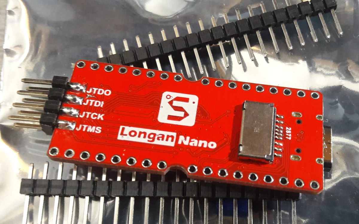
JTAG and SWD are hardware debug interfaces that give direct halt, single-step, and memory read/write access to a processor core. When they are left enabled, they are the most powerful foothold on a board: you can stop the CPU, read and write its RAM and internal flash, and watch keys move through registers. Manufacturers often leave the bare pads on the PCB even after removing the connector, as on the labelled JTDO/JTDI/JTCK/JTMS row pictured.
What it is
JTAG (IEEE 1149.1) was designed for boundary-scan board testing but doubles as a CPU debug port. It is a synchronous serial interface: TCK (clock), TMS (mode select), TDI (data in), TDO (data out), and an optional TRST (reset), plus GND and a VTref reference. Devices chain together, so one probe can reach several parts. SWD (Serial Wire Debug) is ARM's two-wire alternative, SWCLK and SWDIO, that reuses the same silicon debug logic over fewer pins; on most Cortex-M parts SWD rides on the TCK and TMS pads, so a single footprint serves both (see the diagram).
Why it matters
An enabled debug port is close to total control of the chip. You can dump internal flash that is otherwise unreadable, halt the core to read secrets out of RAM or registers, set hardware breakpoints on crypto routines, and patch memory to bypass checks. It sidesteps the software attack surface entirely. That is exactly why hardened devices disable it, by blowing a fuse (an ESP32 JTAG_DISABLE eFuse) or setting a read-out protection level (STM32 RDP level 2). Finding the pads still live is often the whole game.
How to attack it
- Find the cluster. Look near the MCU for a group of 4 to 6 pads or vias, sometimes an unpopulated 2x5 or 1x6 footprint. Silkscreen labels (
TDO,TCK) are a gift; often there are none. - Identify the pinout. With no labels, a
JTAGulatoror a logic analyzer works out which pad is which by driving patterns and watching the IDCODE come back.VTrefandGNDring out with a multimeter. - Connect a probe. A J-Link, ST-Link, or an FT2232-based adapter, driven by OpenOCD, speaks both JTAG and SWD.
- Halt and dump.
# Scan the chain / confirm the target is alive.
openocd -f interface/jlink.cfg -f target/stm32f1x.cfg

# From the OpenOCD telnet/gdb console: halt, then read internal flash.
halt
dump_image flash.bin 0x08000000 0x40000
If the read comes back all 0xFF or errors out, read-out protection or a debug-disable fuse is likely set, and you pivot to fault injection, side-channel, or other angles.
Pitfalls
- Disabled ports look dead. No IDCODE does not always mean "no JTAG"; it can mean the port is fuse-disabled or RDP-locked. Confirm the pads are the debug port before concluding they are not.
- Level and VTref. Drive the probe at the target's logic level and wire
VTrefso the adapter matches; the wrong level gives flaky or no connection. - Pin ambiguity. Guessing the pinout by hand is slow and can short signals. Use a JTAGulator or analyzer rather than brute-forcing with power applied.
- One glitch can brick. Writing flash or fuses over the debug port is as irreversible as any other write. Read first; write only when you understand the effect.