JTAG/SWD probe
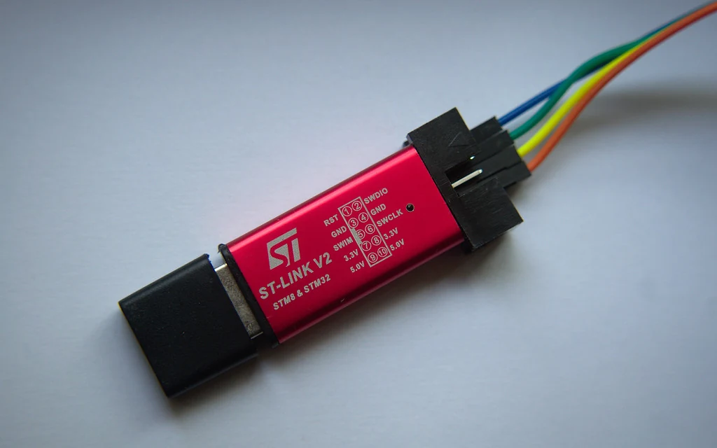
What it does
JTAG and SWD are hardware debug interfaces that give direct halt, single-step, and memory read/write access to a processor's core. An enabled debug port is total control: dump internal flash, bypass readout protection, patch RAM, and read keys live. A cheap ST-Link covers SWD on ARM parts; an FT2232H-based adapter drives full JTAG for a wider range of chips.
Use cases
Halt the core and read out the microcontroller's own flash, bypassing whatever the running firmware would show you.
Some read-out protection levels can be downgraded through a defined (if destructive) debug sequence.
Attach GDB through the probe to set breakpoints and inspect registers live.
How you use it
Find the port (JTAGulator brute-forces an unknown pinout), connect a probe, then bridge it to GDB with OpenOCD:
openocd -f interface/stlink.cfg -f target/stm32f1x.cfg
# in another shell, via the telnet console on :4444
halt
dump_image firmware.bin 0x08000000 0x10000
Wiring
All-0xFF or all-0x00 dumps. That pattern usually means read-out protection (RDP/CRP) is active, not that the wiring is wrong.
Match interface and target configs. OpenOCD needs the right interface and target .cfg pair or the scan chain is never found.